Youth Of Nagaland To Actively Participate In National Service
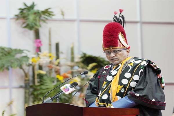
Vice President C. P. Radhakrishnan has called upon the youth of Nagaland to actively participate in national service and contribute to nation-building, stating that a Viksit Nagaland will play an important role in achieving a Viksit Bharat. Addressing the 8th Convocation Ceremony of Nagaland University at Lumami in the Zunheboto district today.
The Vice President emphasised that unity remains India’s greatest strength despite its vast diversity. The Vice President also highlighted the transformative infrastructural development and peace initiatives witnessed in the North-East region over the past decade under the leadership of Prime Minister Narendra Modi.
Referring to the Frontier Nagaland Territorial Authority agreement, he noted that peace and cooperation are crucial for the overall development of the state. The Vice President, who is on a three-day visit to the Northeastern states of Nagaland, Mizoram and Tripura, will leave for Aizawl tomorrow.(UPDATED ON 6TH MARCH 2026)